Any object, whether natural or not, has essential features that can range anywhere between millimeters to nanometers. For example, if we want to study a computer chip, we need to get a 3D view of its overall structure as well as its integrated circuits – and we need to do that without destroying it.
However, there is currently no single platform that can do all of that. Scientists and engineers have to use multiple imaging systems with different imaging capabilities, which can be labor-intensive, time-consuming, and generally limiting.
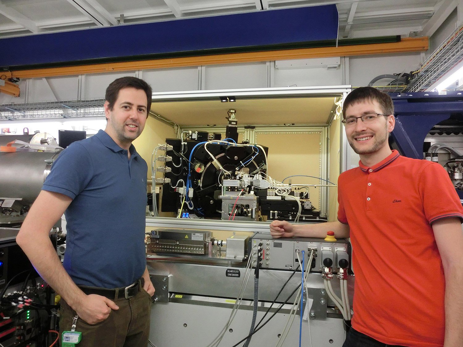
Ideally, we would need a probe, like a microscope, that is capable of “zooming” seamlessly between the macro- and nano-scale, producing 3D low-resolution overviews as well as high-resolution close-ups. This is exactly what researchers from the Paul Scherrer Institute have built, working with colleagues in the US. The study is reported in Nature Electronics.
The new probe is based on an imaging technique now called “ptychographic X-ray laminography”. Ptychography generates microscopic images by “seeing” how it scatters x-rays at varying sample positions. Laminography is similar to X-ray tomography, but is specialized to flat surfaces like printed circuit boards.
[ad_336]
By combining the two methods into a single platform, the researchers show its performance in producing 3D images of an integrated circuit manufactured in 16 nm FinFET technology. The imaging was carried out at the Swiss Light Source SLS of the Paul Scherrer Institute.
The researchers built the tested chip specifically with security applications in mind.
“There is a particularly urgent need to validate chips that have been produced in foundries outside the oversight of the firms that design them,” says Aeppli. “This has been particularly highlighted by the possibility of subtle hardware ‘backdoors’ inserted during remote manufacturing, which would compromise the security of networked information processors.”
[rand_post]
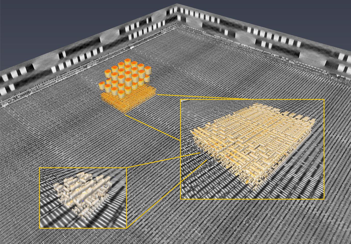
To demonstrate the platform’s “zoom feature” the team first produced a low-resolution overview scan covering a large region of 300 x 300 µm2. They then “zoomed” into a much smaller part of the area covering a field-of-view diameter of 40 µm, and were able to image it at a 3D resolution of 18.9 nm – and all without needing to do anything else to the sample and staying in the same instrument.
“We determined the detailed geometry of the functional features of the chip,” says Mirko Holler, the PSI scientist who led the project, “and were able to perform the “needle in a haystack” search for a particular logic circuit – called an “inverter” – which was present at only one location in the scanned area of the chip.”
The imaging technique is not limited to integrated circuits, but can be used for high-resolution 3D imaging of any flat extended samples, which appear throughout science and engineering.