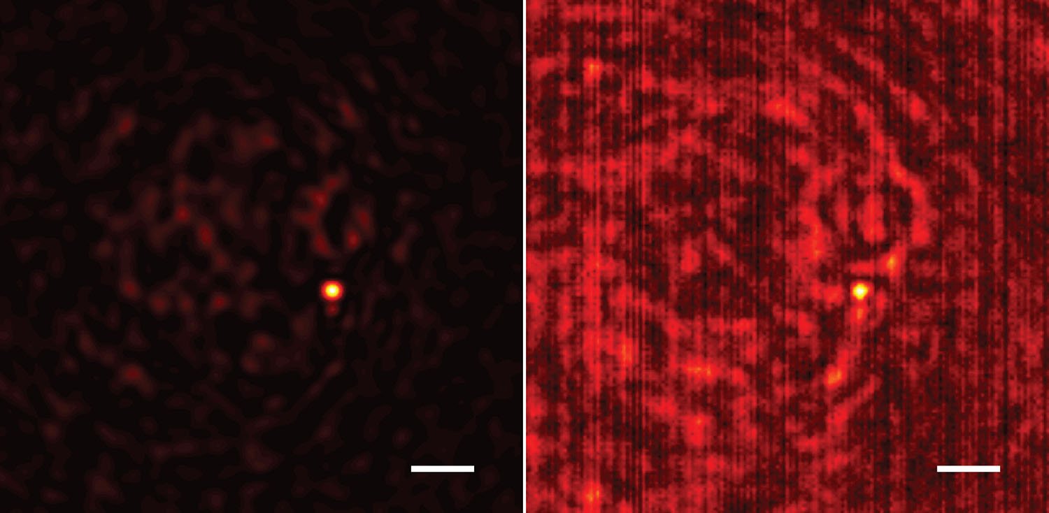
A team led by scientists at the University of Washington has designed and tested a 3D-printed metamaterial that can manipulate light with nanoscale precision. As they report in a paper published Oct. 4 in the journal Science Advances, their designed optical element focuses light to discrete points in a 3D helical pattern.
The team’s design principles and experimental findings demonstrate that it is possible to model and construct metamaterial devices that can precisely manipulate optical fields with high spatial resolution in three dimensions. Though the team chose a helical pattern – a spiral helix – for their optical element to focus light, their approach could be used to design optical elements that control and focus light in other patterns.

Devices with this level of precision control over light could be used not only to miniaturize today’s optical elements, such as lenses or retroreflectors, but also to realize new varieties. In addition, designing optical fields in three dimensions could enable creation of ultra-compact depth sensors for autonomous transportation, as well as optical elements for displays and sensors in virtual- or augmented-reality headsets.
“This reported device really has no classical analog in refractive optics – the optics that we encounter in our day-to-day life,” said corresponding author Arka Majumdar, a UW assistant professor of electrical and computer engineering and physics, and faculty member at the UW Institute for Nano-Engineered Systems and the Institute for Molecular & Engineering Sciences. “No one has really made a device like this before with this set of capabilities.”
The team, which includes researchers at the Air Force Research Laboratory and the University of Dayton Research Institute, took a lesser-used approach in the optical metamaterials field to design the optical element: inverse design. Using inverse design, they started with the type of optical field profile they wanted to generate – eight focused points of light in a helical pattern – and designed a metamaterial surface that would create that pattern.
“We do not always intuitively know the appropriate structure of an optical element given a specific functionality,” said Majumdar. “This is where the inverse design comes in: You let the algorithm design the optics.”
[ad_336]
While this approach seems straightforward and avoids the drawbacks of trial-and-error design methods, inverse design isn’t widely used for optically active large-area metamaterials because it requires a large number of simulations, making inverse design computationally intensive.
Here, the team avoided this pitfall thanks to an insight by Alan Zhan, lead author on the paper, who recently graduated the UW with a doctoral degree in physics. Zhan realized that the team could use Mie scattering theory to design the optical element. Mie scattering describes how light waves of a particular wavelength are scattered by spheres or cylinders that are similar in size to the optical wavelength. Mie scattering theory explains how metallic nanoparticles in stained glass can give certain church windows their bold colors, and how other stained glass artifacts change color in different wavelengths of light, according to Zhan.
“Our implementation of Mie scattering theory is specific to certain shapes – spheres – which meant we had to incorporate those shapes into the design of the optical element,” said Zhan. “But, relying on Mie scattering theory significantly simplified the design and simulation process because we could make very specific, very precise calculations about the properties of light when it interacts with the optical element.”
Their approach could be employed to include different geometries such as cylinders and ellipsoids.
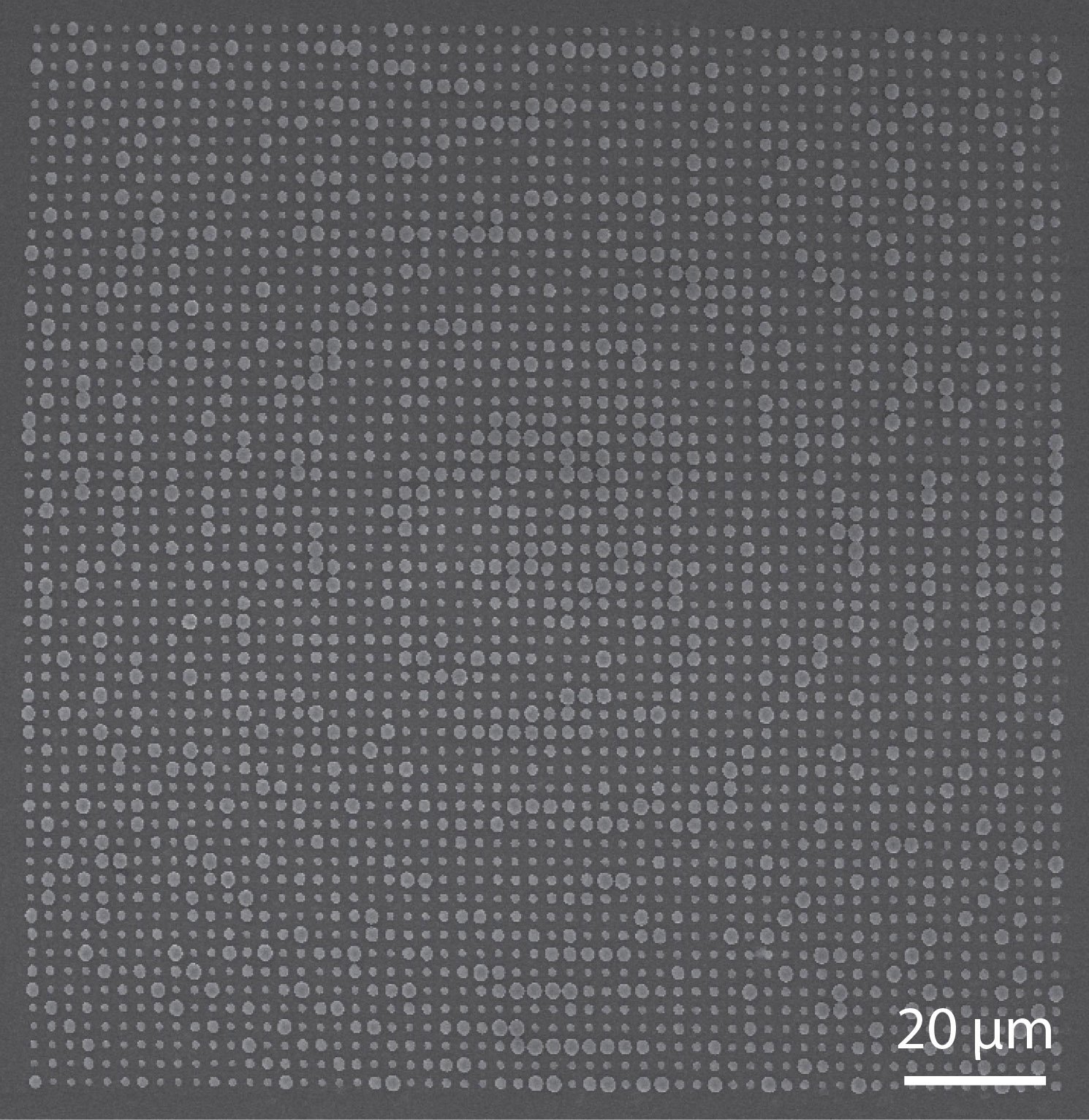
The optical element the team designed is essentially a surface covered in thousands of tiny spheres of different sizes, arranged in a periodic square lattice. Using spheres simplified the design, and the team used a commercially available 3D printer to fabricate two prototype optical elements – the larger of the two with sides just 0.02 centimeters long – at the Washington Nanofabrication Facility on the UW campus. The optical elements were 3D-printed out of an ultraviolet epoxy on glass surfaces. One element was designed to focus light at 1,550 nanometers, the other at 3,000 nanometers.

The researchers visualized the optical elements under a microscope to see how well they performed as designed – focusing light of either 1,550 or 3,000 nanometers at eight specific points along a 3D helical pattern. Under the microscope, most focused points of light were at the positions predicted by the team’s theoretical simulations. For example, for the 1,550-nanometer wavelength device, six of eight focal points were in the predicted position. The remaining two showed only minor deviations.
[rand_post]
With the high performance of their prototypes, the team would like to improve the design process to reduce background levels of light and improve the accuracy of the placement of the focal points, and to incorporate other design elements compatible with Mie scattering theory.
“Now that we’ve shown the basic design principles work, there are lots of directions we can go with this level of precision in fabrication,” said Majumdar.
One particularly promising direction is to progress beyond a single-surface to create a true-volume, 3D metamaterial.
“3D-printing allows us to create a stack of these surfaces, which was not possible before,” said Majumdar.