A team of scientists has collected experimental evidence indicating that a large concentration of electron pairs forms in a copper-oxide (cuprate) material at a much higher temperature than the “critical” one (Tc) at which it becomes superconducting, or able to conduct electricity without energy loss. They also detected these pairs way above the superconducting energy gap, or a range of energies that electrons cannot possess.
Their results, published today in the journal Nature, may point at a way to boost the superconducting properties of cuprates and to find new – and perhaps better – high-temperature superconductors (HTS). While cuprates and other HTS become superconducting at unusually high temperatures compared to conventional superconductors, they still require expensive cooling with liquid nitrogen to operate. Research aimed at understanding the mechanism behind high-temperature superconductivity could help scientists further raise Tc to an economically practical level at which large-scale applications, such as lossless power lines across the electric grid, could be enabled.
“If you don’t know where to look, the phase space is infinite,” said co-corresponding author Ivan Bozovic, group leader of the Oxide Molecular Beam Epitaxy Group in the Condensed Matter Physics and Materials Science (CMPMS) Division at the U.S. Department of Energy’s (DOE) Brookhaven National Laboratory and professor of applied physics at Yale University.
“Our measurement spectra directly revealed a high percentage of electron pairs well above the expected temperature and energy ranges. The exciting prospect now is to leverage this knowledge to enhance superconductivity in cuprates by chemically or physically tweaking some parameters, or to search for other strange metals in which such pairs could exist.”
A mysterious electronic state
In the textbook explanation of superconductivity, electrons spinning in antiparallel directions (think of two little magnets, one pointing north and the other south) pair up at and below Tc, collectively condensing into a “superfluid” that flows freely without resistance. But cuprates do not conform to this picture. For one, their “normal” (non-superconducting) and superconducting states do not resemble those of conventional metals and superconductors. In particular, their density of states (DOS) – the number of electrons for a given volume at a given energy level – is different. For the normal state of ordinary metals, the DOS is constant. Once the metal goes superconducting below Tc, a suppression in the DOS develops at low energy levels – the so-called superconducting (energy) gap. Unexpectedly, in cuprates, such a DOS depression is observed even at temperatures well above Tc, even though the material is not superconducting.
“This so-called “pseudogap” has been one of the main mysteries related to cuprates and HTS for the past 30 years,” explained Bozovic. “Many proposals have been put forward to explain its nature and origin. One picture is that the pseudogap is characterized by a formation of electron pairs. In our previous comprehensive studies of the key physical properties of cuprate superconductors, we presented experimental results supporting this scenario. However, the evidence was circumstantial, so we decided to test the theory directly by measuring the charge of mobile carriers in the pseudogap.”

Charge measurements
Most of the available methods to make this measurement involve nanostructuring the material – for example, as very small dots or wires – through a patterning technique called electron-beam lithography. However, because of the short coherence length of electron pairs (distance between the two electrons), these methods require devices that are sized on the scale of a few nanometers.
“Nobody to this day has been able to do lithography on this scale on cuprates and keep them superconducting,” said Bozovic.
One method that does not require nanolithography is to take “shot noise” measurements in tunnel junctions, which are electronic transport devices that sandwich a thin layer of an insulating material in between two thicker layers of electrically conducting materials (top and bottom electrodes). When current is run vertically, electrons can tunnel (jump) across the insulating layer from one electrode to the other.
[ad_336]
“If you have a statistical process like shooting a dart at a dart board, not all of the darts will hit in the same place,” explained Bozovic. “They will be spread out, showing some distribution. Analogously, if we very precisely measure the direct current flowing through a conductor, we will observe that the current varies with time in a random manner, even if only slightly. In this study, the statistical fluctuations are in electric current when the electrons transport through the device. The current does not continuously flow like a waterfall. Instead, the number of electrons passing through varies with time, showing a characteristic distribution. These deviations from the average current are called the shot noise, which directly reveals the charge of the carriers.”
The challenge is that in order to measure the shot noise, you need to restrict the current to be very low (otherwise these deviations may be hard or impossible to detect). The thin insulating layer can act as a barrier to provide this restriction.
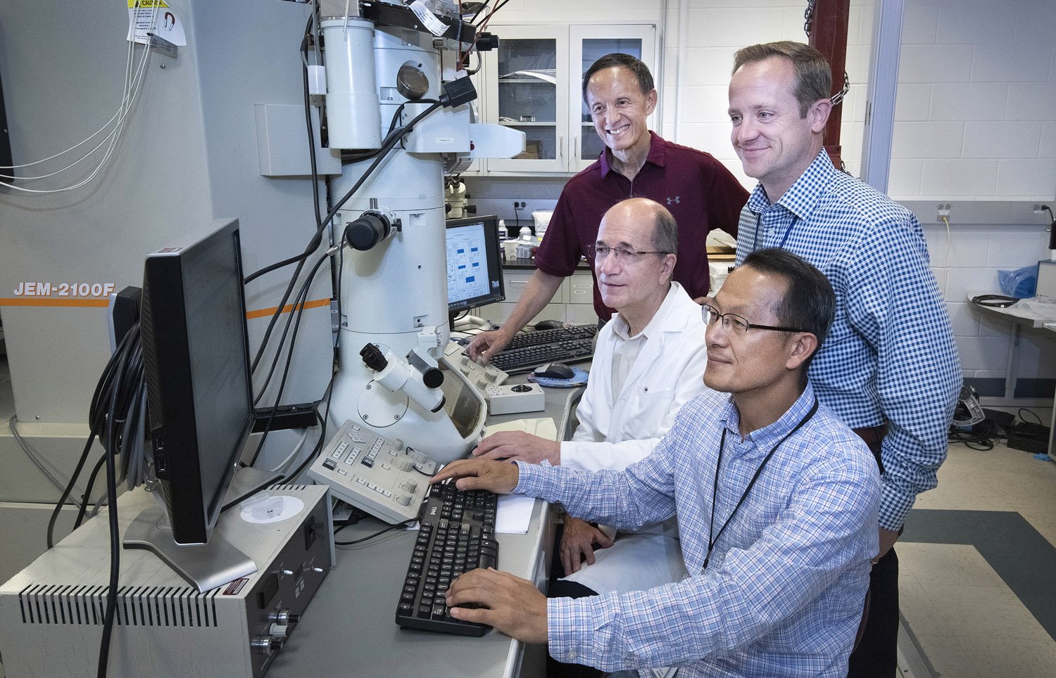
In this case, the scientists built tunnel junctions with a nine-atom thick insulating layer made of lanthanum copper oxide in between two thicker superconductor layers made of lanthanum strontium copper oxide. To make the three-layered structures, they used a sophisticated synthesis technology called layer-by-layer molecular beam epitaxy, which Bozovic and his group have been perfecting at Brookhaven for nearly two decades. This fabrication is technically very challenging because superconductivity decays very close to the surface of cuprates. Thus, atomically smooth surfaces are required; otherwise, imperfections would kill the tunneling current. The scientists verified that the interfaces were atomically perfect by imaging the structures and mapping their elemental composition with advanced electron microscopy and spectroscopy techniques developed by co-author Yimei Zhu -a physicist and leader of the Electron Microscopy and Nanostructure Group in Brookhaven’s CMPMS Division – and his group members.
“The diameter of our tunnel junction devices is not nanometers – one-billionth of a meter – but micrometers,” said Bozovic. “Lithography is much easier to do on this larger scale.”
The scientists then measured the current-voltage characteristics of the fabricated devices over a range of temperatures, energies (voltages), and doping concentrations (dopants are elements added to a material to alter its electronic properties). They performed the measurements at Brookhaven; Rice University, where professor Douglas Natelson and his group used high-precision shot noise instrumentation; and the University of Connecticut, where professor Ilya Sochnikov used an ultracold refrigerator to access the lowest temperatures possible. For all three independent measurements, the scientists obtained plots with the same curves.
[rand_post]
The shot noise spectra directly showed that, in these cuprate devices, preformed pairs exist well above the Tc and superconducting energy gap. The lower the doping level is, the higher the percentage of pairs.

“Our results have profound implications for basic condensed matter physics theory,” said Bozovic. “In some sense, the textbook chapters have to be rewritten. From this study, it appears that we have a new type of metal, in which a significant fraction of the electrical current is carried by electron pairs. On the experimental side, I expect that this finding will trigger much follow-up work – for example, using the same technique to test other cuprates or superconductors, insulators, and layer thicknesses.”