In “Avengers: Endgame,” Tony Stark warned Scott Lang that sending him into the quantum realm and bringing him back would be a “billion-to-one cosmic fluke”.
In reality, shrinking a light beam to a nanometer-sized point to spy on quantum-scale light-matter interactions and retrieving the information is not any easier. Now, engineers at the University of California, Riverside, have developed a new technology to tunnel light into the quantum realm at an unprecedented efficiency.
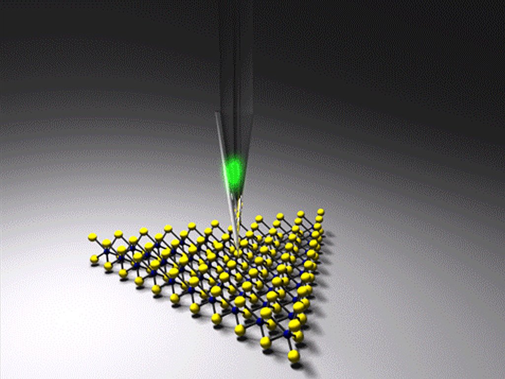
In a Nature Photonics paper, a team led by Ruoxue Yan, an assistant professor of chemical and environmental engineering, and Ming Liu, an assistant professor of electrical and computer engineering, describe the world’s first portable, inexpensive, optical nanoscopy tool that integrates a glass optical fiber with a silver nanowire condenser. The device is a high-efficiency round-trip light tunnel that squeezes visible light to the very tip of the condenser to interact with molecules locally and send back information that can decipher and visualize the elusive nanoworld.
[rand_post]
Our ability to zoom in on the fine details of an object is limited by the wave nature of light. If you ever used an optical microscope in a science class, you probably learned that one can only magnify an object by about 2,000 times before everything becomes a blur. That’s because it’s impossible to distinguish any features finer than half the wavelength of light — a few hundred nanometers for far-field visible light — no matter how advanced your microscope is.
Unlike far-field waves, near-field waves only exist very close to a light source and are not governed by this rule. But they do not travel voluntarily and are very difficult to utilize or observe. Since the 1920s, scientists have thought that forcing light through a small pinhole on a metal film would generate near-field waves that could be converted to detectable light, but the first successful prototypes weren’t built until half a century later.

In the early 1990s, Eric Betzig, the 2014 Nobel laureate in chemistry, made substantial improvements to earlier prototypes in imaging performance and reliability. Since then, near-field scanning optical microscopy, as the technique is known, has been used to reveal the nanoscale details of many chemical, biological, and material systems.
Unfortunately, almost another half-century later, this technique is still esoteric and used by few.
“Sending light through a tiny pinhole a thousand-times smaller than the diameter of a strand of human hair is no piece of cake,” Liu said.
“Only a few in a million photons, or light particles, can pass the pinhole and reach the object you want to see. Getting a one-way ticket is already challenging; a round-trip ticket to bring back a meaningful signal is almost a daydream.”
Scientists have made endless efforts to improve this chance. While the most sophisticated probes today allow only one in 1,000 photons to reach the object, the UC Riverside device delivers half the photons to the tip.
“The key of the design is a two-step sequential focusing process,” Yan said.
“In the first step, the wavelength of the far-field light slowly increases as it travels down a gradually thinning optical fiber, without changing its frequency. When it matches the wavelength of the electron density wave in the silver nanowire lying on top of the optical fiber, boom! All energy is transferred to the electron density wave and starts to travel on the surface of the nanowire instead.”
In the second step of the focusing process, the wave gradually condenses to a few nanometers at the tip apex.
The UC Riverside device, a tiny silver needle with light coming off the tip “is sort of like Harry Potter’s wand that lights up a tiny area,” explained Sanggon Kim, the doctoral student who carried out the study.
Kim used the device to map out the frequency of molecular vibrations that allow one to analyze chemical bonds that hold atoms together in a molecule. This is known as tip-enhanced Raman spectroscopy, or TERS, imaging. TERS is the most challenging branch of near-field optical microscopy, because it deals with very weak signals. It usually requires bulky, million-dollar equipment to concentrate light and tedious preparation work to get super-resolution images.
With the new device, Kim achieved 1-nanometer resolution on a simple portable equipment. The invention could be a powerful analytical tool that promises to reveal a new world of information to researchers in all disciplines of nanoscience.
“The integration of a fiber-nanowire assembly with tip-enhanced Raman spectroscopy coupled with a scanning tunneling microscope enables the collection of high-resolution chemical images in a simple and elegant setup, placing this tool at the forefront of optical imaging and spectroscopy. We are proud of this achievement and its impact on chemical research. We are even more encouraged by its potential application in a wide array of disciplines such as biological and materials research, which will further scientific advancement,” said Lin He, acting deputy division director for the National Science Foundation Division of Chemistry that in part funded the research.