Nippon Telegraph and Telephone Corporation (NTT, Head office: Chiyoda-ku, Tokyo; President & CEO: Jun Sawada) and Tokyo Institute of Technology (Tokyo Tech, Headquarter: Meguro-ku, Tokyo; President: Kazuya Masu) have demonstrated an ultrafast all-optical switching operation with the lowest energy consumption ever reported for all-optical switching at less than one picosecond (one trillionth of a second). Previously reported all-optical switches would have difficulty operating at such a high speed with low energy consumption.
The current achievement combines an ultrasmall optical waveguide with a height and width of a few dozen nanometers, called a plasmonic waveguide, with graphene, a material that shows great promise for nonlinear optics. Such ultrahigh switching speed cannot be achieved by electrical control. It is expected that this switch will be used in future photonic integrated circuits for ultrafast information processing. In addition, this development shows novel promising possibility for applications of plasmonics.
A report on this development was published online in Nature Photonics on November 25, 2019.
Optical switches will be important components in future photonic integrated circuits for ultrafast information processing. Optical switches control the on/off state or the direction of optical signals, and the switching speed depends on whether the optical signals are optically or electrically controlled. All-optical switches control optical signals with other optical signals, so they are unaffected by the RC time constant, which limits the operation speed of electrical devices. Thus, it has been expected that all-optical switches will operate faster than electrically controlled ones.
[ad_336]
However, the switching energies of the previously reported all-optical switches are relatively large. This energy problem is a critical one for ultrafast information processing because optical components must be densely integrated in photonic circuits and the energy consumption of each device must be low. As shown in Fig. 1, high speed and low energy consumption have not been achieved simultaneously with the previously reported all-optical switches, and it had been assumed that a trade-off existed between the switching energy and switching time.
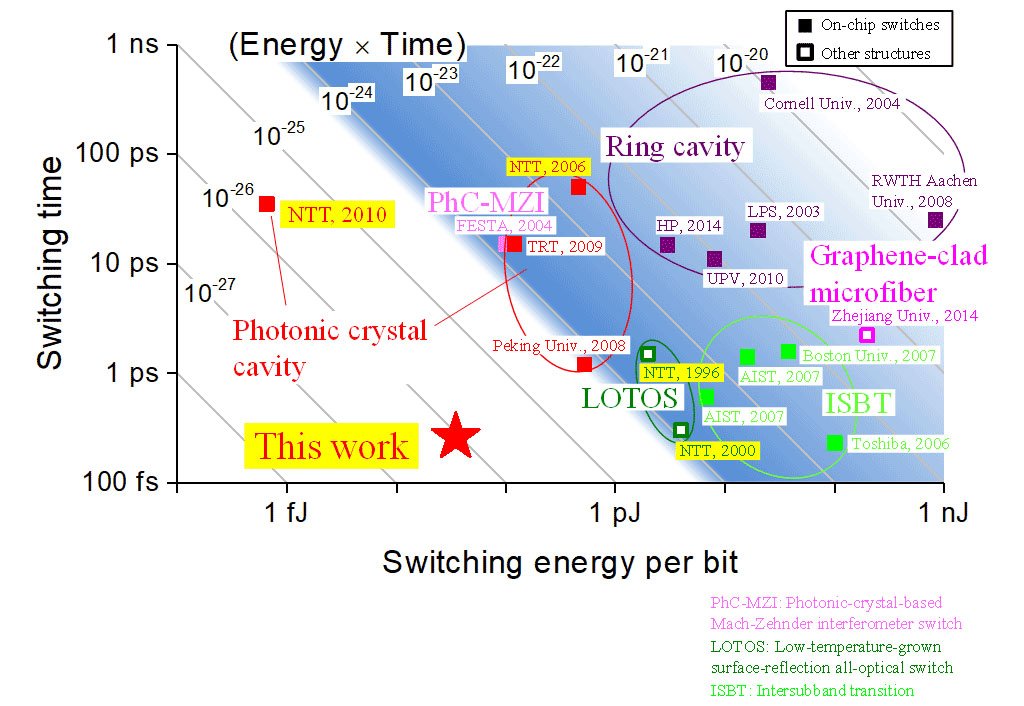
In 2020, however, NTT overcame this trade-off and demonstrated all-optical switching with an extremely small driving energy by using a photonic crystal nanocavity with modest operating speed (tens of picoseconds). On the other hand, the trade-off still remained in the ultrafast switching regime (less than one picosecond), which is beyond the capability of electrical control.
[rand_post]
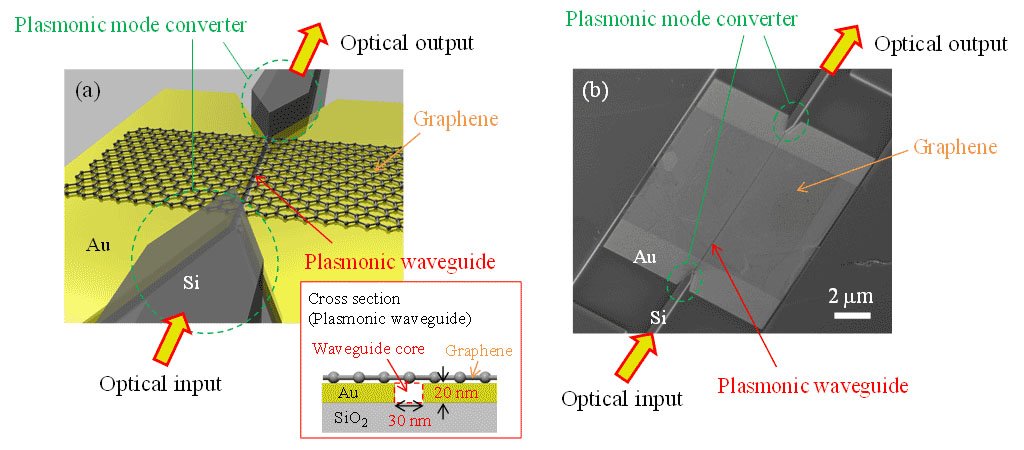
NTT and Tokyo Tech developed an all-optical switch operating in the ultrafast regime (less than one picosecond) with low energy consumption by combining an extremely small optical nanoscale waveguide based on plasmonics with graphene (Fig. 2a). The main points are as follows.
Enhancement of absorption and nonlinear optical effect in graphene with plasmonic waveguides
To control optical signals with other optical signals, the properties of a material placed on the optical path must be changed with light, and the response time (i.e., the time in which this change occurs) is the one of the limitations on the switching time. Here, we employed graphene, which has an ultrafast nonlinear optical response. Graphene is not only a promising for its speed; it also has a large absorption coefficient over a broadband wavelength range. On the other hand, graphene is only one-atom thick, and the interaction with light is weak, which leads to long photonic devices and high energy consumption. In this work, we overcame this problem by strongly confining light within a nanoscale plasmonic waveguide.
[ad_336]
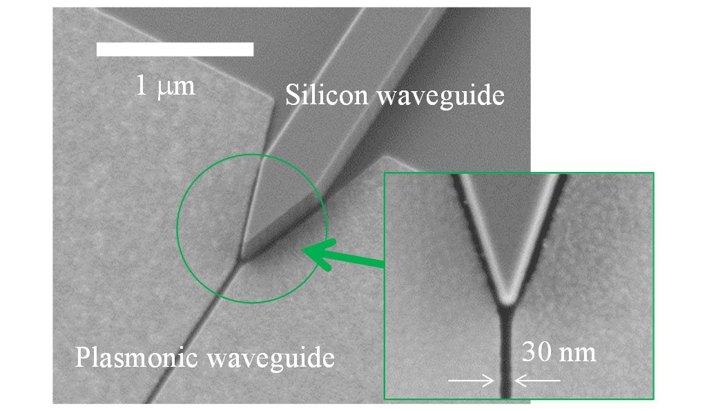
We fabricated small plasmonic waveguides with a core size of 30 nm × 20 nm and loaded graphene on them by using NTT’s nanofabrication technologies (Fig. 2b). The cross-sectional area of these plasmonic waveguides is about 1/100th that of “compact” silicon waveguides and 1/105 that of single-mode optical fibers. It was experimentally shown that the absorption coefficient of the graphene-loaded plasmonic waveguide is one order of magnitude smaller than that of graphene-loaded silicon waveguides. Moreover, the energy required for inducing nonlinear optical effects is four orders of magnitude smaller. These results show that compactness and low energy consumption can be achieved at the same time.
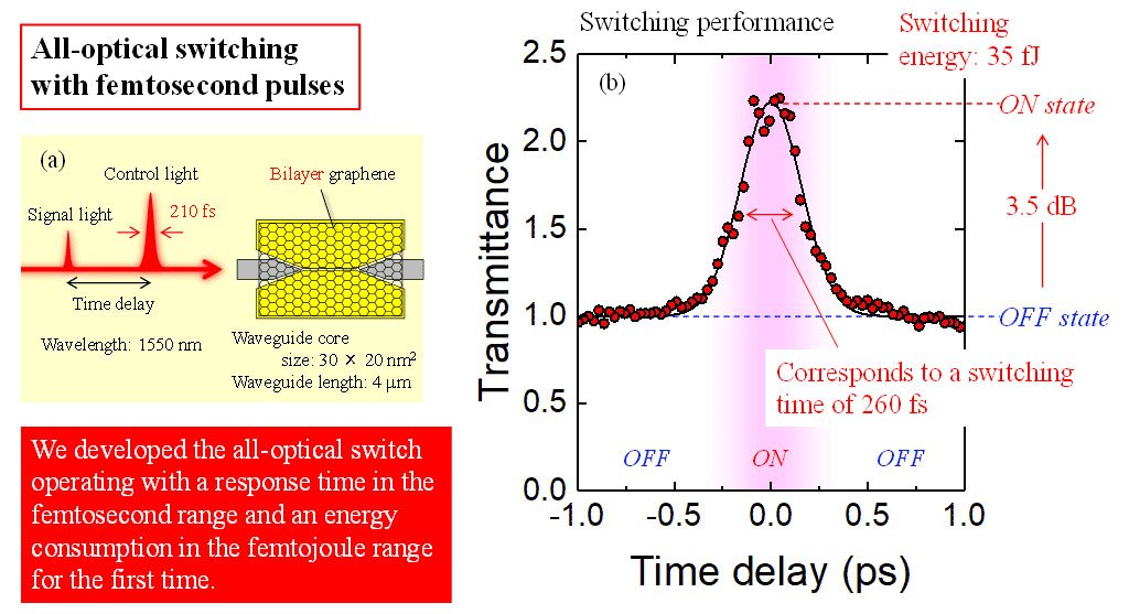
Demonstration of ultrafast all-optical switching
The signal light is switched (on/off) with control light in all-optical switches (Fig. 3a). In our switch, the control light induces a nonlinear optical effect of graphene; i.e., it changes the degree of absorption by graphene. Figure 3b indicates that a switching time of 260 fs can be achieved with a switching energy of 35 fJ. The switching time is one order of magnitude shorter and the energy four orders of magnitude smaller than those of previous graphene-based devices. In addition, as shown in Fig. 1, the switching energy is the smallest value ever reported (1/100th of that previously reported) for any type of all-optical switch operating at less than one picosecond. Thus, we developed the first all-optical switch operating with a response time in the femtosecond range and an energy consumption in the femtojoule range. Moreover, the energy-time product, which is a measure of the trade-off mentioned above, was somewhat improved over that of the previous best device.
NTT and Tokyo Tech are working on overcoming the limitations of electronics, such as on the operation speed and energy consumption, by integrating a dense photonic network into a processor chip. The all-optical switch operates much faster than an electrically controlled one and consumes less energy. We expect that it will be used in future photonic integrated circuits for ultrafast information processing.
As well, the nanoscale waveguide of the switch is a superior platform for developing nanophotonic information processing devices incorporating nanowires and other two-dimensional materials. Moreover, we envision that our device can be used as a nonlinear activation function in optical neural networks. In the future, we will increase the performance of the all-optical switch, apply its technology to other photonic devices such as detectors, and examine the use of other nanomaterials.